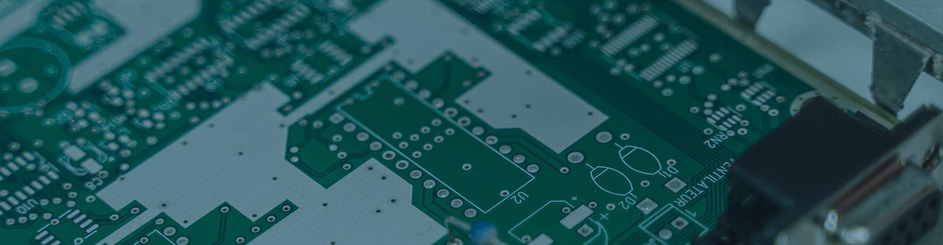
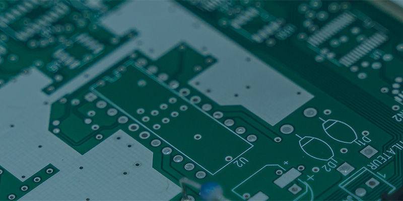
PCB PROFESSIONAL MANUFACTRRER!
PCB PROFESSIONAL MANUFACTRRER!
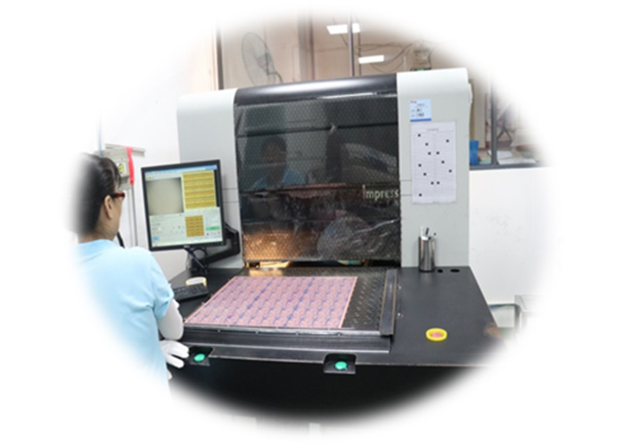
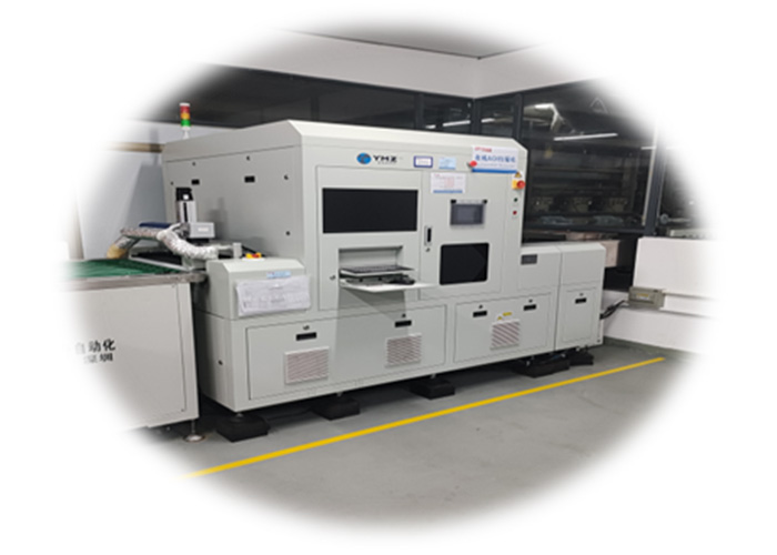
To uphold the highest standards of product quality, our company has made a substantial investment in Automated Optical Inspection (AOI) equipment. AOI technology is critical in the PCB manufacturing process, as it provides precise and consistent monitoring of each board at various stages of production, ensuring that every detail meets our strict quality criteria.
The developing stage in PCB manufacturing is critical because it is during this process that the circuit pattern on the board is formed. Accurate scanning and inspection of the board at this stage are essential to ensure that the integrity of the circuit pattern is maintained and that no defects are carried forward into subsequent processes.
To prevent these issues, an AOI inspection is performed immediately after the developing stage. AOI systems use high-resolution cameras and advanced algorithms to scan the entire surface of the PCB. They meticulously compare the actual circuit pattern against the intended design specifications, identifying even the smallest discrepancies or defects.
To prevent these issues, an AOI inspection is performed immediately after the developing stage. AOI systems use high-resolution cameras and advanced algorithms to scan the entire surface of the PCB. They meticulously compare the actual circuit pattern against the intended design specifications, identifying even the smallest discrepancies or defects.
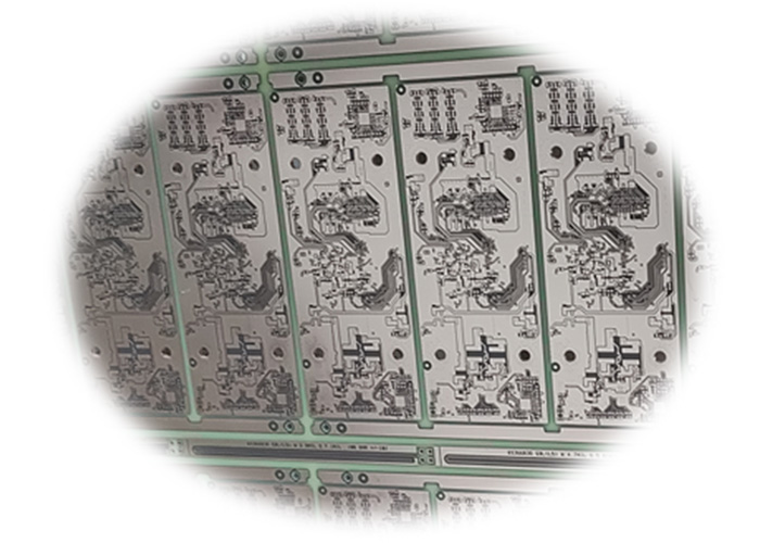
AOI (Automated Optical Inspection) plays a vital role in ensuring the quality and reliability of PCB boards, particularly after the etching process. The etching stage is where the circuit pattern is fully realized, making it a critical point in the manufacturing process.
AOI inspection at this stage allows for a thorough comparison between the actual etched circuit and the customer’s design specifications. The AOI system scans the entire surface of the PCB, using high-resolution cameras and sophisticated software to detect even the smallest discrepancies. This ensures that the circuit pattern aligns precisely with the design intent, meeting all technical requirements.

Tel.: +86 0755 2332 1191
Fax: +86 0755 8176 4499
Add.: Building A1, Zone B, Ditang Industrial Zone, Shasan Community Agricultural Company, Shajing Street, Bao'an District, Shenzhen
Copyright © DICKSON Circuit Shenzhen Co., Ltd. All Rights Reserved | Technical Support: Nbone


 sales@dspcb.com
 +86 13828761409
 CN
CN Home >